The following article which has been edited by “Bojan Stojkovski” (right image) shows that how a new technique can transform several terabytes of microelectronics via a one-millimeter crystal. The article, even copied from the published source, is more completed by addition of extra hyperlinks (shown in BOLD/RED fonts) and extra images (including the image of the editor) by the PIMI’s Editorial-Team.
*****************************************
Researchers at the University of Chicago – (Pritzker School of Molecular Engineering) have developed a method to store data using crystal defects as ones and zeroes, each the size of an individual atom.
UChicago PME Assistant Professor Tian Zhong explained that each memory cell is created from a single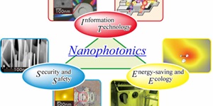 missing atom, or defect. This approach allows terabytes of data to be packed into a small cube of material just a millimeter in size, shows the research published in Nanophotonics.
Quantum methods revolutionize classical computing

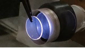
The innovation showcases UChicago PME’s interdisciplinary approach by applying quantum techniques to transform classical, non-quantum computers. It repurposes research originally focused on radiation dosimeters devices (left image) typically used to measure radiation exposure for hospital workers – into revolutionary microelectronic memory storage.
According to first author Leonardo França, a postdoctoral researcher in Zhong’s lab, they integrated solid-state physics used in radiation dosimetry with research focused on quantum science, even though their work is not purely quantum. This interdisciplinary approach enabled the development of groundbreaking  microelectronic memory storage.
The researcher further adds that their work bridges quantum and optical data storage, meeting the need for better quantum systems and improved classical memory storage. The research began during França’s Ph.D. studies at the University of São Paulo in Brazil, where he focused on radiation dosimeters – devices that passively monitor radiation exposure for workers in hospitals, synchrotrons, and other radiation facilities. These materials can absorb radiation and store the exposure information for a specific period.
-
Nanotechnology: A New Frontier Aperture Nanotechnology: A New Frontier -
Ultralight Metallic Microlattices Electron Microscope Hack to see Graphene
França explained that when the crystal absorbs enough energy, it releases electrons and holes, which are then captured by the defects. This information can be read by releasing the electrons and detecting them optically. Recognizing its potential for memory storage, França brought this non-quantum approach to Zhong’s quantum laboratory, leading to the interdisciplinary innovation.


Rare earths enhance memory storage with powerful optical properties
 To develop this innovative memory storage technique, the team incorporated rare earth elements, also known as lanthanides, into a crystal. They specifically used praseodymium and an yttrium oxide crystal, though the process they developed can be applied to a variety of materials, utilizing the powerful and flexible optical properties of rare earth elements.
In contrast to dosimeters, which are activated by X-rays or gamma rays, this storage device is triggered by a simple ultraviolet laser. The laser excites the lanthanides, causing them to release electrons. These electrons are captured by defects in the oxide crystal, such as gaps where a single oxygen atom is missing. The technique leverages these inherent defects, which are found in both natural and artificial crystals.
While crystal defects are commonly used in quantum research to create “qubits,” the UChicago PME team discovered a new application. They successfully controlled which defects were charged and which weren’t, designating charged gaps as “ones” and uncharged gaps as “zeros”, with the innovation transforming the crystal into a highly efficient memory storage device, surpassing previous limits in classical computing.